H8 Parallel/GPIO + WizNET Network/SPI Controller
DISCLAIMER and ATTRIBUTION: Norberto Collado and Douglas Miller have produced a WizNET board that utilizes the ultra-high-speed SPI channels of their WizNET circuit to access SD storage, as an alternative to CF-based H8 storage solutions. The SD storage was not of interest to me at this time, but I did have a desire to retire an 82C55 PPIO board. The current project provides a combination of WizNET, SPI, and parallel/GPIO functions one one board, while eliminating the specialty 82C55 PPIO card from the H8 bus. The WizNET/SPI circuitry of the Collado/Miller board is used with permission in this project, and attribution is noted on the board itself.
This board provides a mix of parallel I/O types for the H8, using 74xx574 output latches, 74xx541 input buffers, and the Microchip MCP23x17 SPI/I2C port expander. It is an alternative to the 82[C]55 boards, and may be simpler to use than the 82[C]55 for typical GPIO functions. The 74xx574 and 74xx541 chips on this board require no setup or initialization - write a byte, read a byte. The 74xx-based ports have optional jumpers between the input and output ports of a pair for readback capability. This makes manipulation of individual bits by independent processes easy, without having to maintain a shadow memory byte. One potential downside of this simple hardware arrangement is that there is no interrupt capability. To handle more sophisticated GPIO requirements, the MCP23S17 16-bit IC is used to provide two additional 8-bit ports. The MCP IC has interrupt capability, bitwise control of I/O direction, optional pull-up resistors, and readback. The MCP23S17 provides GPIO capabilities to the H8 that are very similar to an Arduino or other modern microcontroller. There is an available SPI channel that can be jumper-configured for either 3.3v or 5v operation. All other ports operate with 5v logic. The total I/O capacity of the board is 24 x 5v digital input, 24 x 5v digital output, and 16 x 5v bidirectional GPIO.
H8 backplane space is often at a premium, so to leverage available real estate this board includes the H8xSPI / WizNET controller circuit designed by Douglas Miller and Norberto Collado. The implementation of their circuit on this board does not include the SD storage access that is on their newest standalone WizNET board. The WizNET portion of the circuit on this board is identical to that of the standalone WizNET board, so the WizNET software developed by Douglas runs on this board without modification. The WizNET GAL from the standalone board is also used, with slight modification for the buffered (and inverted) address lines present on this board. Simple mechanical changes were made to the layout of the generic SPI features of the board, making it a little easier to use the SPI channels for purposes other than WizNET. A few scope or logic probe test points have been provided to explore the SPI functions. It should be noted that the discrete hardware used in this SPI circuit is an EXTREMELY high performance SPI channel. It requires no hardware polling between OUTputs, even with Z80 block I/O instructions. It runs at CPU bus speed, and has been tested up to 16MHz with the WizNET module. There is no faster SPI implementation possible within the H8 architecture - the circuit delivers data to the SPI channel as fast as the CPU can provide it. If you have slower SPI devices (sensors, for example) that can't tolerate such high clock rates, take a look at this I2C<->SPI bridge that provides the H8 with an SPI channel that operates with a less stratospheric clock.
The MCP23S17 chip (SPI channel "C") can be optionally designated as a parallel printer port. No hardware jumpers are needed - just plug in a standard IBM PC parallel printer cable. If you don't want to use the parallel printer functionality, just leave the 26-pin connector empty. Starting with the MX80 parallel print driver from Glenn Roberts as a base, the 8255-specific code was modified to work with the MCP23S17 port expander on this card.
A note about output port chip selection. Beyond simplification of I/O functions, one of the motivations behind this board was to get increased current handling on individual output bits compared to the 82[C]55. The datasheet current limitation for each output pin on the 82[C]55 is just 2.5ma (sink or source). That's not enough to safely drive even a single LED without an external buffer. I know - people do it all the time. There are plenty of circuits out there that show 8255s wired direct to all manner of output devices requiring source/sink well in excess of 2.5ma. To each his own. I specified 74ALS574 devices for this board, which are readily available and can safely sink 24ma or source 3ma - plenty to control LEDs or a bunch of TTL loads. 74LS574 devices have similar current capabilities, but are difficult to find from first-tier sources. The 74HCT574 chip is generally available and specified at 6ma sink/source, so it could also be used as long as the datasheet current loads are respected. If you need more output current capacity, you could use the 74AS574, which can sink a whopping 48ma or source 15ma. The downside of the 74AS574 is its cost - about five times the cost of the ALS device. Lines on the MCP23 ports have an absolute maximum rating of 25ma source/sink, although the recommended current is 8ma sink, 3ma source. Any of the ports can easily directly operate an LED.
GPIO speeds: The four ports using 74xx logic can operate at 16MHz and are the fastest channel for bit-hungry parallel I/O applications. The MCP23 chips are rated at 10MHz SPI. Writing a byte to or reading a byte from the serial-attached chips requires transfer of at least three bytes (device address, register number, and value) over the selected serial channel. This cannot be as fast as direct byte-wise I/O on the 74xx ports, but it's still usually much faster than the attached peripheral. While the datasheet specifies a maximum SPI clock speed of 10MHz for the MCP23S17, I have run it at 16MHz/3.3v continuously for hours with no glitches. YMMV - that 16MHz result may well be chip dependent.
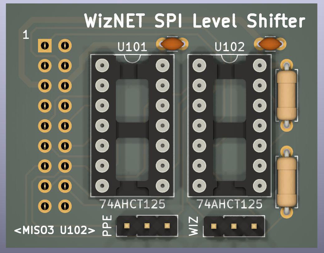
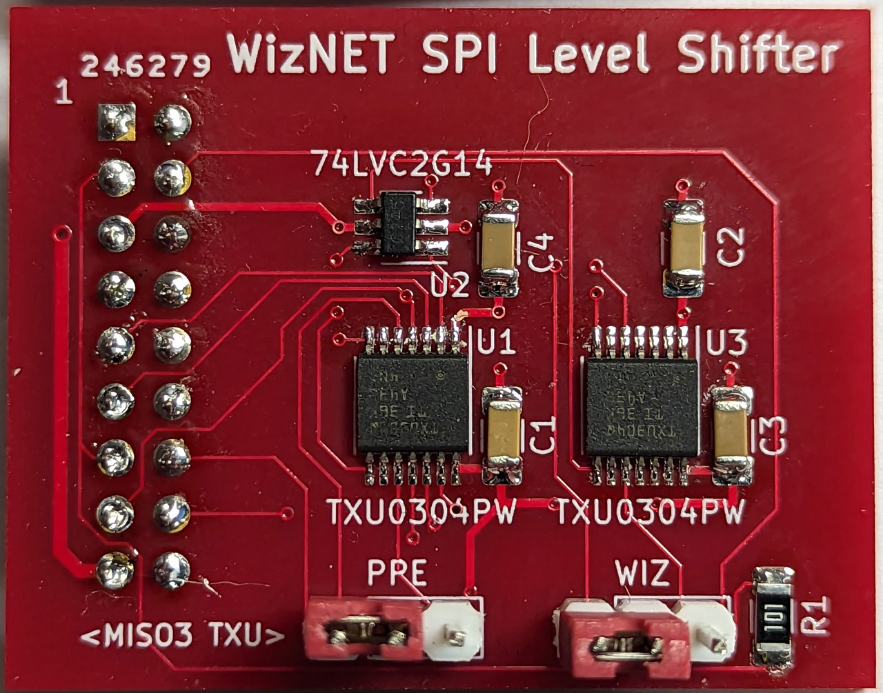
A note about the external SPI channels on this board: Headers are provided for optional level shifting between 5v and 3.3v using a small daughtercard. Daughtercards using the TI TXU0304 or 74LV125/74AHCT125 chips have been produced. Note that the SPI clock on this board is taken from the H8 bus clock, so the slowest possible SPI clock rate is 2MHz. If you have slower SPI devices, you may want to consider the above mentioned I2C<->SPI bridge. Cabling to an off-board SPI device must be kept (very) short to avoid compromising the clock signal.
Board construction: This board has been prototyped as both a 4-layer board (SIGNAL-GROUND-GROUND-SIGNAL) and a 6-layer board (SIGNAL-GROUND-SIGNAL-SIGNAL-GROUND-SIGNAL) stackup. Although 16MHz is at the (very) low end of computer high frequencies, the layout of this board respects many of the design issues for high speed circuits. Many of the layout ideas used on this board came from Eric Bogatin's "Practical Guide to Prototype Breadboard and PCB Design" and "Signal and Power Integrity Simplified". Texas Instruments Application Note SPRAAR7J "High Speed Interface Layout Guidelines" was also helpful.
| Stub circuits were eliminated from critical circuits where that was reasonably possible - signal traces daisy chain through all their connections without forming "T" or "Y" paths. | |
| Layer changes (front to back) were minimized. Where a via had to be used, a grounding via was placed nearby to assure a good ground return path. The 6-layer design has no layer changes for any signal trace. | |
| Signal layers are adjacent to their reference ground plane. | |
| (Some) bypassing is done with 1uf or 10uf ceramic capacitors. | |
| Series resistors were used in critical high-speed signal lines (like the bus and SPI clock) to minimize ringing and overshoot. The resistance value used was determined by varying the resistance while observing the waveform, and optimizing for the cleanest signal possible. Typical resistances are ~47 ohms. Below, you will find photographs of the signal traces that show the significant improvement in waveform possible by adding series resistance. |
16MHz operation: "F" family devices are specified for components that are in critical time paths for the SPI channel. "ALS" devices could also be used. With "LS" devices, the acumulated propagation delays are too great to support 16MHz running. Look here for information about a post-prototype change that was found to be necessary to reliably run SPI at 16MHz.
*UPDATE (May 18, 2023): I am no longer pursuing the version of this board that includes an 8255.
| Schematic | Board X-Ray View | Bill of Materials (pdf) | Bill of
Materials (HTML interactive) |
| Schematic: TXU0304 shifter | WinCUPL GAL Source | Jumper Settings | |
| Schematic: 74xx125 shifter | |||
| MCP23x17 Datasheet | SPI MOSI Timing |

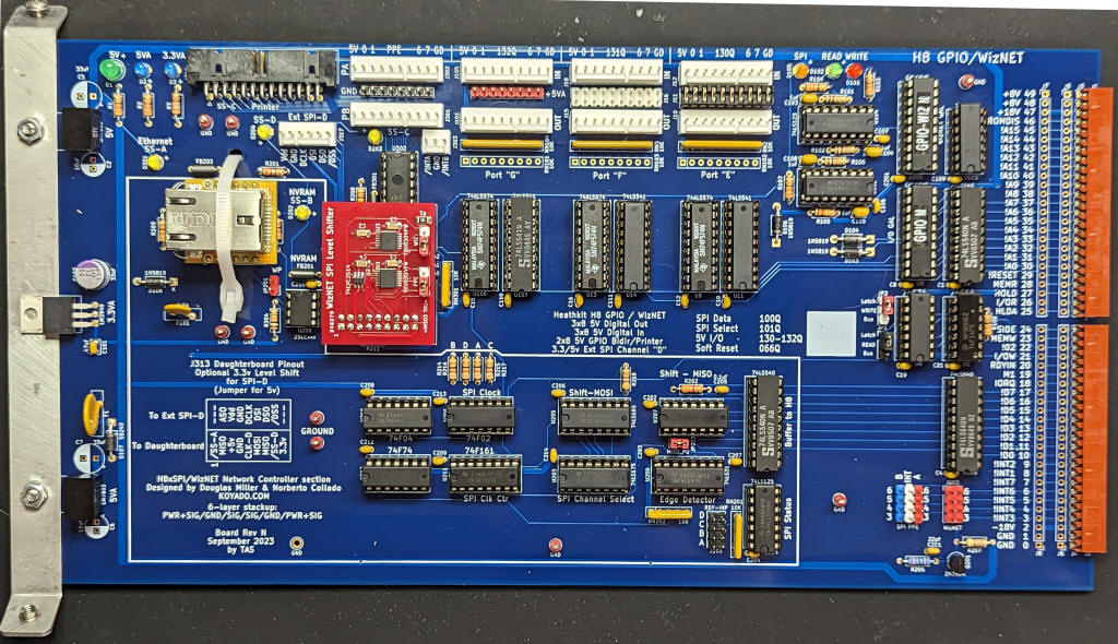
Above: Assembled board with 3.3v daughtercard installed. This is a 6-layer board design.

Above: Detail of daughterboard installation for 3.3v voltage translation. Separate daughtercards for 74AHCT125, TXB0104, and TXU0304 have been produced. The TXU0304 is ideally suited for SPI level translation, but has had limited availability in a TSSOP SMD package. The TXU0304 is not dynamically bidirectional like the TXB0104. It has three fixed A->B channels (for SCLK, MOSI, SCS) and one fixed B->A channel (for MISO). This configuration is a perfect match for the requirements of 4-wire SPI communications.
Final SPI Waveforms:
 |
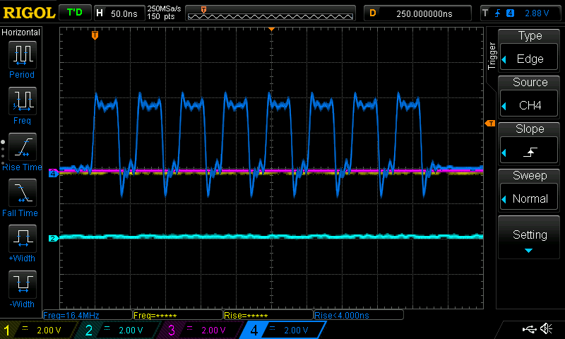
SPI MOSI waveform at 16MHz, measured at external headers |
 |
SPI MISO waveform at 16MHz, measured at external headers |
Source Series Resistance Experiments:
Adding series resistance is often prescribed for taming ringing or overshoot. To test this method, I observed the SPI clock signal (16MHz) while varying the series resistance with a 200 ohm trimmer pot. The traces were taken at U206 pin 1.
 |
This is the SPI CLK signal with no series resistance.
Overshoot on falling edge is quite high (nearly -2 volts).
Disclaimer #1: While this signal doesn't look very good, the circuit operates just fine at 16MHz. Disclaimer #2: How do I know that I am not just observing artifacts introduced by stray capacitance or inductance on my scope probes? While I can't guarantee that I am not significantly altering the signal with my test equipment, I have observed the waveform after putting a seccond probe on the line in parallel with the first. I observe a very slight reduction in ampltude with two probes connected, but the basic character of the waveform does not change at all. I would expect that if the probe is introducing significant capacitance or inductance, a second probe would show a marked change in waveshape. Since it does not, I conclude that my measurement equipment is probably not significantly altering the signal under test. |
 |
This is the SPI CLK signal at maximum resistance (200 ohms). The falling edge has been cleaned up, but the overall wave form has been significantly rounded with extended rise and fall times. |
 |
Here is the waveform after adjusting the trimmer for the best "flat
line" top and bottom of the clock square wave. The overshoot on
the falling edge has been completely eliminated. The waveform is
visually crisp, but rise and fall times have been lengthened slightly.
To my eye, this is preferable to the 2v overshoot on the falling edge. The resistance required to produce this waveform was 74 ohms. A 75 ohm fixed resistor was put in the circuit, and the final waveform matched this test trace exactly. |
 |
Three daughtercards for 5v->3.3v level shifting of SPI channel "D". TOP: TXB0104 breakout from Adafruit MIDDLE: TXU0304 BOTTOM: 74AHCT125 or 74LV125
|
 |
 |
| ABOVE: 74AHCT125 or 74LV125 shifter BELOW: TXU0304 shifter |
|
 |
 |