Propagation Delays on the Parallel to Serial Shift Register for the SPI MOSI Circuit
After very occasionally encountering SPI errors at 16MHz during long-term use of the board, I started looking carefully at some timing constraints. During initial board design, it was noted that the accumulated propagation delay through "LS" technology components wasn't fast enough to handle switching of a 16MHz clock. To resolve that issue, several of the ICs in the WizNET circuit were specified as "F" family devices with much lower propagation delays than "LS" devices. During long-term testing of the board, I still very occasionally encountered 16MHz errors with SPI. The discussion below shows what I found when looking further into timing issues associated with the remaining "LS" family devices in the SPI circuit.
Shift register 74xx165 at U205 converts parallel data from the H8 bus to a serial data stream for the SPI MOSI signal. The SPI devices sample the serial data on the rising edge of the clock, while the shift register clocks the data out on the falling edge (the clock signal to the shift register is inverted by U210D). Assuming a completely symmetrical clock signal at 16MHz, this allows just 31.5ns between the "clock out" signal to the shift register and the "clock in" to the SPI device. There are three timing components that must be considered:
| Delay Element | Datasheet Typical (ns) |
Datasheet Maximum (ns) |
| PD through 74F04 U210D | 3.5 | 5 |
| PD through 74LS165A (clock to serial data) | 15 | 25 |
| setup time for SPI device (WizNET module) | 3 | 3 |
| Total PD plus setup | 21.5 | 33 |
Ouch! Devices operating at the datasheet maximums will fail to meet the setup requirements of the WizNET module.
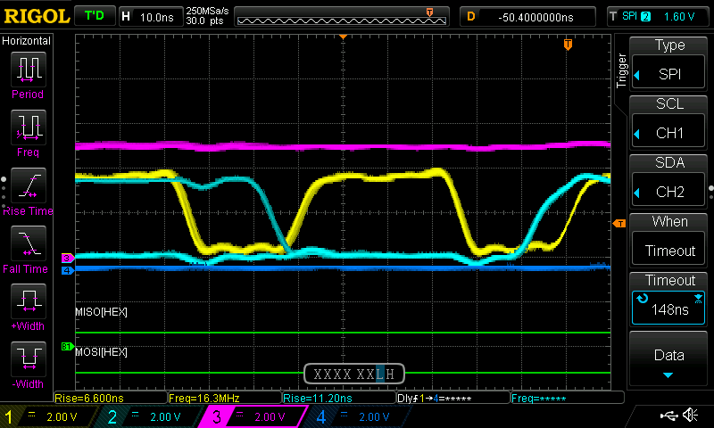
The initial design for this board uses a 74F14 inverter for the bus control signals, including the clock. The 74LS14 is often used on H8 boards to improve the noise margin on the bus control signals. But the built-in hysteresis of the Schmitt trigger results in an asymmetric clock, where the "clock low" portion of the waveform has a shorter duration than the "clock high". In other words, the time between the falling and rising edges of the clock is less than the time between the rising and falling edge. This reduces the available window for the serial clock output from 31.5ns to less than 25ns (see scope traces) making it even more likely that there will be occasional errors due to missing the setup time requirements.
The solution to this timing issue was two-fold. First, the 74LS165A was replaced with a 74ALS165, which has a PD at least 10ns better than the LS chip: 3ns (typical), 14ns (maximum). As can be seen in the scope traces below, just making this substitution brings the transitions on MOSI well ahead of the setup time requirement. Secondly, the 74F14 at U1 was replaced with a 74F04. This restores the fully symmetric clock, adding even more margin to the MOSI signal. The scope traces below show the improvement in setup time margin that was possible with these two changes. This does reduce the noise immunity on the IOWR and IORD bus signals however.
 |
With 74LS165A Shift Register and 74F14 Control Buffer Yellow: SPI
Clock At 16MHz, the falling edge of MOSI is 3-4ns ahead of the rising edge of the clock at a 1.5v threshold. That is dangerously close to the 3ns setup time requirements of the WizNET module. It explains why there had been some occasional SPI errors, and some sensitivity to chip selection during initial testing. Notice how the SPI clock is asymmetric, with an "ON" time of about 38ns and an "OFF" time of about 24ns. A perfectly symmetrical clock would have ON and OFF = 31.5ns. This shortening of the "OFF" time pushes the MOSI transitions up against the rising clock, encroaching on the setup time.
|
 |
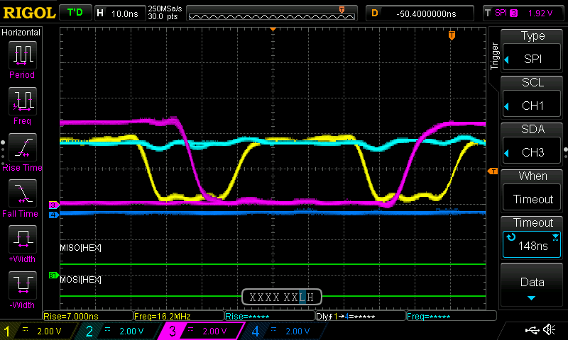
With 74LS165A shift register Yellow: SPI Clock At 16MHz, transitions on the MISO signal generated in the WizNET module are at least 12ns ahead of the rising clock transition. So the timing issues are limited to MOSI. Another example of the asymmetric SPI clock caused by the 74F14 used to buffer the bus control signals. |
 |
After replacing shift register with 74ALS175 Yellow: SPI Clock Even with the asymmetric clock, MOSI transitions are now well outside the setup time threshold, occurring about 16ns ahead of the rising clock. This is perfectly consistent with datasheet "typical" values, which are about 10ns faster with the ALS family component. |
 |
After replacing 74F14 bus control buffer with 74F04 Yellow: SPI
Clock With the symmetrical SPI clock restored, the setup time margin has improved even further. MOSI transitions are now about 20ns ahead of the rising clock. This waveform shows a very clean and almost perfectly symmetrical clock, with clean MOSI transitions occurring well before the minimum setup time.
NOTE: For the particular components installed on the test board, making either of these changes alone would have resolved the setup time crunch. But it's important to note that if installed components approach datasheet maximum values, the "LS" family shift register is not fast enough to meet the WizNET setup requirements even with a fully symmetrical clock. Both ICs (74LS165A shift register and 74F14 bus control buffer) should be swapped to guarantee stable operation in all circumstances. |
 |
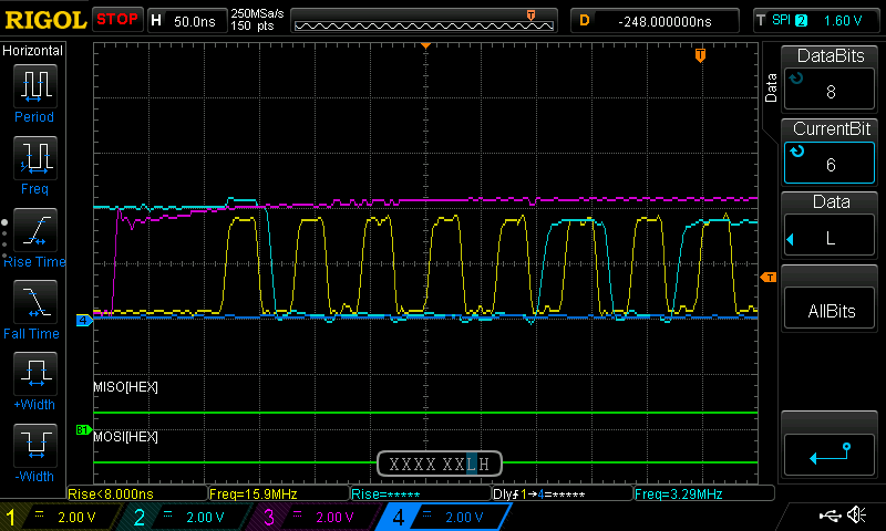
Final MOSI waveform check after replacing both ICs. Yellow: SPI
Clock This trace shows a complete byte ('10000101b') sent over SPI at 16MHz. The series resistors on the clock and MOSI lines have damped ringing and overshoot. The circuit has nice clock symmetry, and MOSI transitions have ample setup time margin. |